NXP’s MCX A5 Cortex-M33 MCUs bring 10BASE-T1S Ethernet and post-quantum crypto to the edge
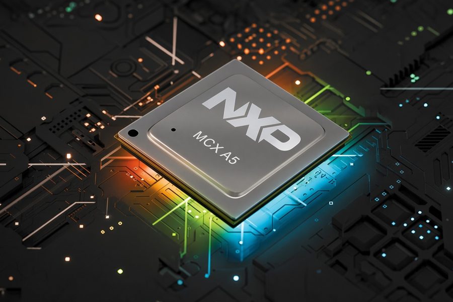
NXP has unveiled the MCX A5 family of microcontrollers built around the Arm Cortex-M33 core, targeting industrial and networking applications such as programmable logic controllers, remote I/O modules, building and energy management systems, and other connected edge devices. The new MCUs run at up to 240 MHz and come with up to 2 MB of dual-bank Flash memory with ECC and read-while-write support, along with 640 KB of SRAM.
A standout feature of the MCX A5 series is its integrated 10/100 Mbps Ethernet MAC paired with a built-in digital PHY for 10BASE-T1S Single Pair Ethernet. This eliminates the need for external PHY chips and enables networking over a single twisted pair, which simplifies cabling and reduces cost in industrial environments. The MCUs also include a wide range of communication interfaces and analog peripherals for flexible system integration.
On the security front, NXP equipped the MCX A5 with an EdgeLock accelerator, secure boot with hybrid post-quantum cryptography (PQC) support, secure firmware update mechanisms, lifecycle management, secure debug, external Flash encryption, and anti-tamper monitoring. The Cortex-M33 core itself includes an FPU, DSP, MPU, and TrustZone technology, and is paired with a SmartDMA co-processor that offloads data movement tasks for improved efficiency. The MCU delivers 988.8 CoreMark points (4.12 CoreMark/MHz), positioning it for real-time control and edge processing workloads.