Home lab builds working LEDs from scratch — a step toward DIY chip bonding
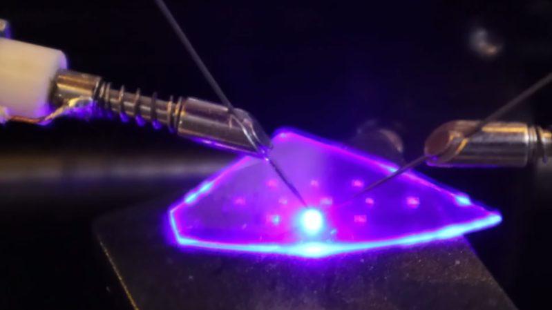
While amateur semiconductor fabrication is often limited to proof-of-concept demonstrations, one enthusiast known as Dr. Semiconductor is pushing the boundaries much further. He is actively developing a method to bond homemade chips to printed circuit boards — a critical step for practical applications. To test the alignment process, he fabricated and successfully bonded transparent LED chips.
The starting material was a gallium nitride (GaN) LED epiwafer on a sapphire substrate. This structure consists of n-doped GaN, an indium gallium nitride quantum well layer, and p-doped GaN. When current flows through the stack, electrons from the n-type layer and holes from the p-type layer recombine in the quantum well, emitting blue light.
To make a functional LED, electrical contacts were needed on both the n-type and p-type layers. Reaching the n-type layer required cutting through the p-type and quantum well layers. Traditionally, this is done with reactive ion etching using chlorine gas. However, Dr. Semiconductor devised an alternative process: a 355-nanometer ultraviolet laser breaks down GaN into gallium and nitrogen, and the resulting cut is cleaned with a potassium hydroxide etch.
For the metal contacts, he applied a photoresist mask, deposited nickel, silver, and titanium in a sputtering chamber, and then dissolved the mask to lift off unwanted metal. The finished LED chips were then soldered onto a PCB.
This work shows that hobbyist-level semiconductor fabrication can go beyond simple demonstrations and move toward creating functional, bonded devices — potentially opening the door to custom chips made at home.