Laser-Carved Paper Circuits Hit 250 µm Resolution and Decompose in Soil
Researchers have proposed a new way to build flexible electronic circuits on a paper substrate, bypassing the main limitation of such devices—low printing accuracy. Instead of traditional wax masks, the authors used hydrophobic parchment paper and a 50-watt CO2 laser that etches channels for conductive inks by removing the silicone coating.
This approach achieved a resolution of about 250 µm for line widths and 300 µm for line spacing. That is noticeably better than wax-based methods, which suffered from the absorbent and uneven structure of cellulose, limiting the sharpness of printed traces. Paper remains an attractive substrate for electronics due to its low cost and easy recyclability, but its use was previously held back by the imprecision of conductor deposition.
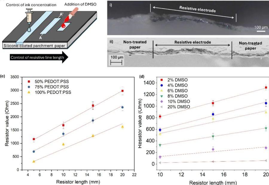
Importantly, the inks in such circuits do more than just form traces—they also create functional components. Conductivity comes from the polymer PEDOT:PSS, and when mixed with dimethyl sulfoxide, it forms resistors. To make capacitors, the researchers printed interlocking PEDOT:PSS "fingers" and covered them with a polyvinyl alcohol-based gel acting as an electrolyte. Using these elements, the authors built RC low-pass and high-pass filters.
Degradation of these papertronic circuits was also tested: samples were buried in soil under typical conditions, where almost all components decomposed except for the silicone coating. Since silicone is chemically and biologically inert, its residual presence is not considered a problem. However, if slower decomposition is desired, encapsulating the device in polydimethylsiloxane (PDMS) is offered as an option.