China builds key EUV lithography laser — ex-ASML engineer lends a hand
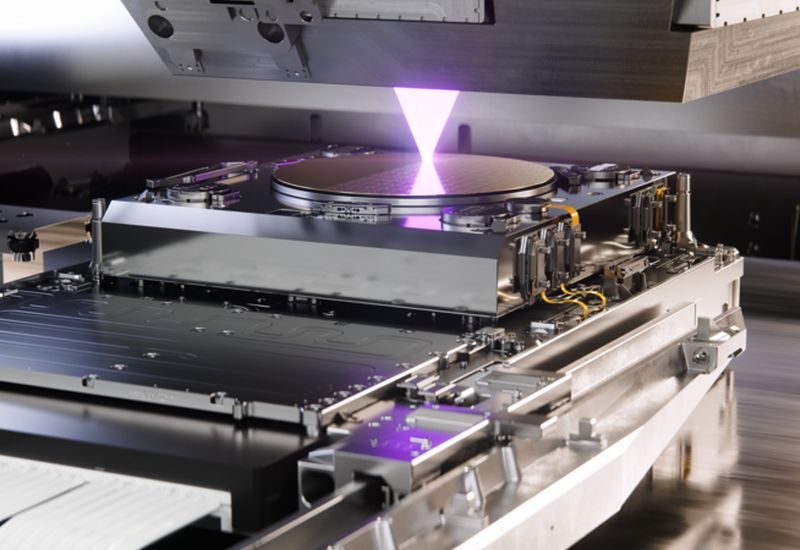
Chinese researchers have succeeded in developing a laser light source in the extreme ultraviolet (EUV) range, a key component for building lithography scanners. This brings China closer to producing chips with process nodes below 7 nm, though experts say years of work remain before full-scale production equipment becomes available.
Until now, such systems were only accessible to chipmakers in the United States, South Korea, and Japan. Shipments of this equipment to China have been banned since 2019 — restrictions were introduced by the Dutch authorities, where the headquarters of ASML, the leading supplier of lithography scanners, is located, and later joined by the U.S. government.
According to Newsbit, a former ASML engineer named Lin Nan, who specialized in developing such lasers while working in the Netherlands, contributed to the creation of the promising light source. Earlier Chinese experimental setups demonstrated an efficiency of no more than 3.42% — meaning only that share of energy was converted into useful radiation. That is acceptable for laboratory conditions but unsuitable for mass production.
Power is another issue. Current Chinese sources deliver between 100 and 150 W, while modern production EUV systems operate at around 600 W. ASML, for its part, plans to raise the power of its sources to 1,000 W, which directly affects the number of chips produced per unit of time.
However, even a successful light source does not solve all the problems. A complete EUV system requires complex mirror assemblies, precision drives, and accompanying software. According to Reuters, prototypes of Chinese EUV scanners still suffer from insufficient optical quality. According to some estimates, a working scanner of Chinese design may not appear before 2028 or even 2030.